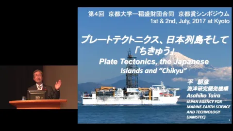
4th Kyoto University-Inamori Foundation Joint Kyoto Prize Symposium
http://kuip.hq.kyoto-u.ac.jp/
https://ocw.kyoto-u.ac.jp/en/opencourse-en/181
July 2, 2017
[Materials Science and Engineering]
Hideo Ohno
Director, Professor, Research Institute of Electrical Communication, Tohoku University
Title of Presentation
“Spintronics -From Synthesis of III-V Magnetic Semiconductors to VLSI Applications-”
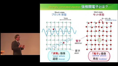
I have been engaged in the study of spintronics for nearly 30 years. Spintronics refers to “electronics utilizing the spin property of electrons.” Magnets, whose properties have been known since the times of the ancient Greeks and Chinese, are typical examples of material in which an orderly state of aligned spins exists. Used in electric motors and for non-volatile recording of data on hard disks, magnets are essential materials in today’s world.
While the properties of a magnet are inalterable once it is made, the resistance of a semiconductor, another essential material in today’s world, can subsequently be electrically altered. Finding potential ways to bridge the gap between these two types of materials was what I had in mind when embarking on my studies.
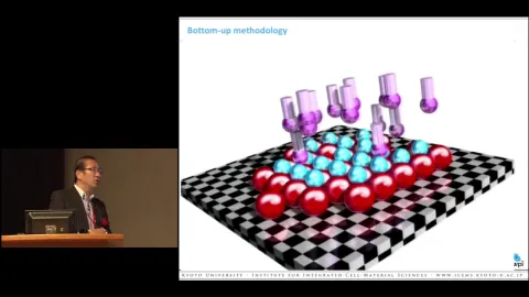
I first took a path in that direction whilst working in the laboratory of then IBM fellow Dr. Leo Esaki as a visiting scientist for 18 months, starting in 1988. Together with a group member at IBM, I set the objective of my research there to create a magnetic material using a group III-V compound semiconductor, a type that was increasingly being utilized in devices. Fortunately, we succeeded in synthesizing (In,Mn)As, a mixed crystal not found in nature, comprising a group III-V compound semiconductor, InAs, and a magnetic atom, Mn. We also discovered through applying a variety of growth conditions that it could be magnetized in low temperatures to become a ferromagnetic semiconductor.
I further pursued this theme at Tohoku University, where my initial activity was a research collaboration with Dr. Tomasz Dietl from Poland which demonstrated, by means of a theoretical model, carriers’ contributions to ferromagnetic phase stability. This opened up the possibility of electrical control of magnetic properties (or spin) because carrier concentrations can be electrically controlled. After overcoming some technical challenges, control of ferromagnetic properties using field effects at the interface between an insulator and a semiconductor was achieved. A series of experiments further demonstrated that the ferromagnetic phase transition temperature of a ferromagnetic material can be controlled through varying the number of carriers using electrical fields and that important properties of a magnet, such as coercivity and magnetic anisotropy, are modulated via spin-orbit interaction.
Starting with creation of a material, we ultimately demonstrated that properties of a magnet can be controlled even after it is made. Our results inspired a number of researchers to broaden the scope of research to metal magnetic materials. Now, energy-efficient non-volatile memory devices are being developed which utilize electric field-controlled magnetization switching.
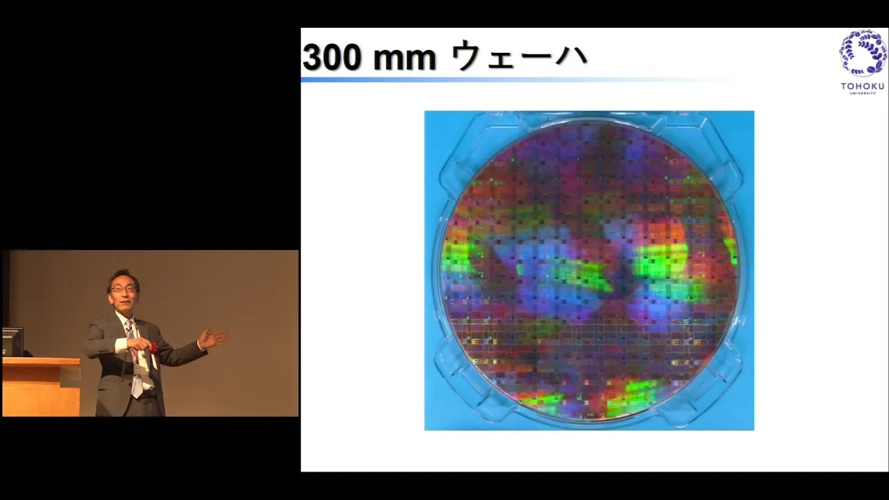
The series of studies also led to the invention of a device with potential for various applications. This discovery came about during the process of applying electric field control to metallic materials. To enable electric field control, the ferromagnetic metal material needs to be a film as thin as several nanometers of thickness. With regard to a key combination for application — namely, CoFeB (magnet) and MgO (insulator) — with an ultra-thin CoFeB film, the perpendicular magnetic anisotropy at the interface between the insulator and the ferromagnetic metal successfully induced a perpendicular magnetization easy axis, which would be essential for realizing a high-performance device. Shortly thereafter, we fabricated a 40-nm scale microscopic spintronic device called a magnetic tunnel junction (MTJ) device, and we published the results after verifying that high performance had been achieved. That was in 2010. Today, the device structure has become a global standard and is widely used in spintronic devices for integrated circuits.
My presentation will also touch on some episodes for the purpose of sharing with the audience the excitement and dynamism of our research activities.
この動画は、クリエイティブ・コモンズ・ライセンス“Attribution-NonCommercial-ShareAlike (CC BY-NC-SA)”が付与されています。 私的学習のほか非営利かつ教育的な目的において、適切なクレジット表記をおこなうことで、共有、転載、改変などの二次利用がおこなえます。 コンテンツを改変し新たに教材などを作成・公開する場合は、同じライセンスを継承する必要があります。 詳細は、クリエイティブ・コモンズのウェブサイトをご参照ください。